| Photo | 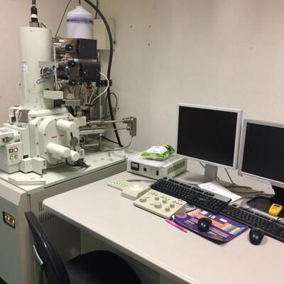 |
| Title | Cold Field Emission Scanning Electron Microscope |
| Purpose | 1. Observation of Surface Structure (SEI, BEI) 2. EDS Elemental Analysis |
| Brand | JEOL |
| Model | JSM-7500F |
| SPEC |
1. Resolution: 2. Accelerating voltage range: 0.1–30 kV 3. Electron gun: Cold Field Emission Electron Gun |
| Sample & Fee |
Training Fee (NT$/person) – 600 Certification Fee (NT$/person) – 300 Operated Fee (NT$/hr) – 600 Sample Platinum Coating: NT$300/time EDS measurement: NT$600 for ≤15 points; for >15 points, NT$200 per additional point |
| Reminder |
1. Samples must not be magnetic, volatile, or corrosive. 4. Starting from September 1, 2009, the Field Emission Scanning Electron Microscope (FE-SEM) is prohibited from imaging polymer materials to avoid equipment damage. If this is not reported in advance, imaging will be immediately stopped, and a NT$1,500 start-up maintenance fee will be charged. |
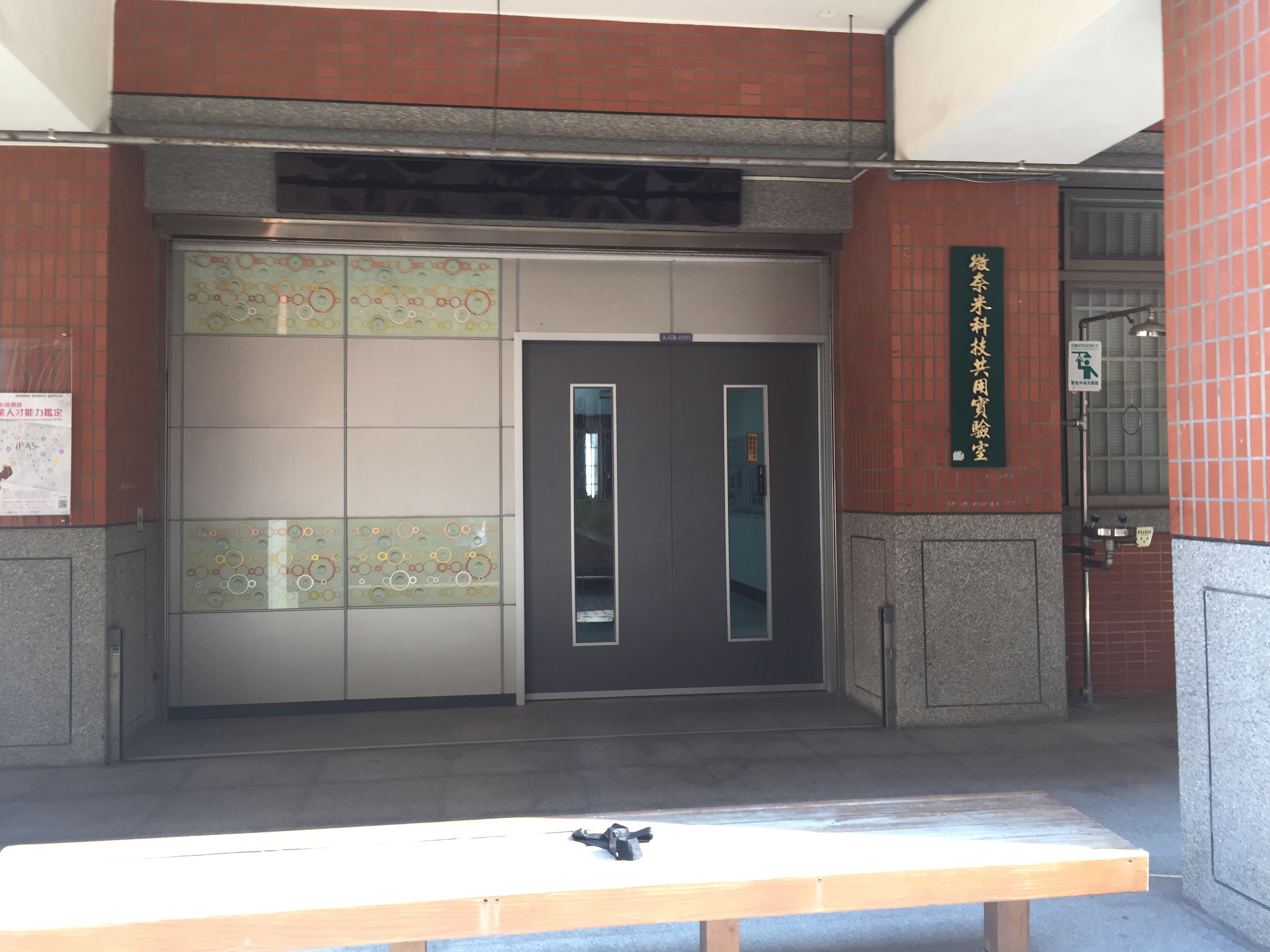
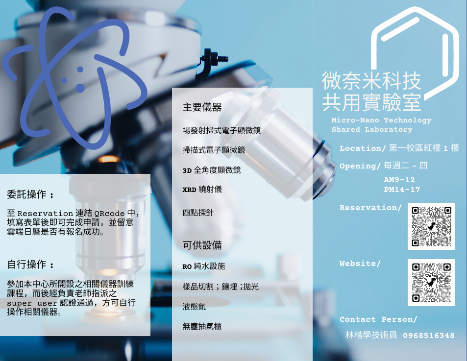
| Location | Red Building 1F, Shared Micro-Nano Technology Laboratory |
| Update | 2019/04/23 |
| Lab | Micro-Nano Technology Shared Lab |
| Hashtags |
View count:
25
